2.1mA Low Current SK6803MINI-EA-002 3228 GRB 4 Feet Smart LED Chips 2000pcs/pack
Product Specification
Product Identification
| Product Model | SK6803MINI-EA-002 |
|---|---|
| Version No. | A/2 |
| Sending Date | 2026-01-07 |
Before using this product, please verify that you are referring to the latest version of this specification.
If special requirements are needed, please contact the relevant engineering personnel.
Contents
- Product Overview
- Main Applications
- Product Naming
- Mechanical Dimensions
- Pin Description
- PCB Recommended Pad Layout
- IC Absolute Maximum Ratings
- RGB LED Optoelectronic Parameters
- IC Electrical Characteristics
- Controller Recommended Data Timing
- Data Transmission Method
- Timing Waveforms
- 24-bit Data Structure
- Typical Application Circuit
- Photoelectric Characteristics
- Packaging Standards
- Reliability Testing
1. Product Overview
- Forward voltage: 5 V @ 2.1 mA (OUT GRB)
- Typical viewing angle (50%): 120°
- Lens color: translucent
- Built-in reset circuit, LEDs remain off at power-on
- Grayscale adjustment: 256 levels
- Single-wire return-to-zero code transmission protocol, infinitely cascadable
- Data transmission frequency up to 800 Kbps; at 30 fps refresh rate, cascade length < 1024 pixels
- Moisture sensitivity level (MSL): 5a
- ESD level: 4 kV (HBM)
- RoHS and REACH compliant
2. Main Applications
- Consumer electronics
- Gaming and e-sports related products
- Light strips, modules, and custom-shaped lighting products
3. Product Naming
Example: SK6803MINI-EA-002
| Position | Description |
|---|---|
| ① | Series – default: RGB LED chip integrated with IC |
| ② | IC series and current code – “6803”: 6803 series IC, 2.1 mA current version |
| ③ | Package outline – “MINI-EA”: 3.2 × 2.8 × 1.78 mm |
| ④ | Internal code – “002” |
4. Mechanical Dimensions
Units: mm, unless otherwise specified. Dimensional tolerance: ±0.1 mm.
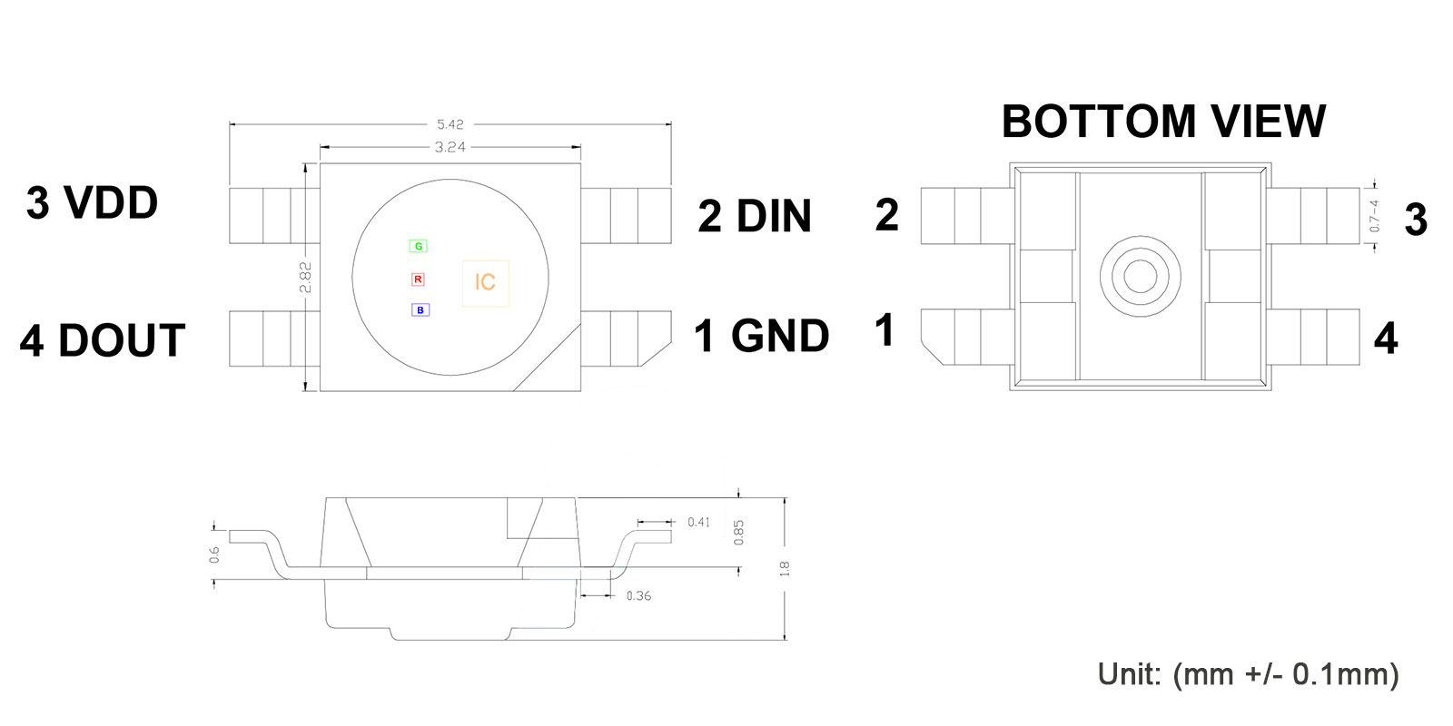
For precise mechanical design, refer to the original dimension drawing with all coordinates and pad locations.
5. Pin Description
| Pin No. | Symbol | Name | Description |
|---|---|---|---|
| 1 | GND | Ground | Power ground |
| 2 | DIN | Data input | Control data signal input |
| 3 | VDD | Power supply | Power supply pin |
| 4 | DOUT | Data output | Control data signal output |
6. PCB Recommended Pad Layout
Units: mm. The following is a logical representation of the recommended land pattern.
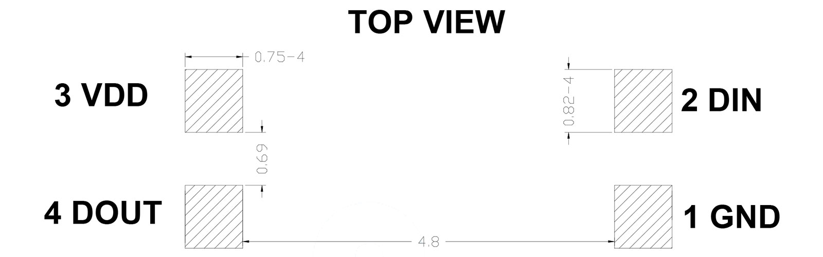
PCB pad dimensions should follow the original recommended drawing to ensure proper soldering and reliability.
7. IC Absolute Maximum Ratings (Ta = 25°C)
| Parameter | Symbol | Range | Unit |
|---|---|---|---|
| Working voltage | VDD | +3.7 ~ +5.5 | V |
| Operation temperature | Topt | -40 ~ +80 | °C |
| Storage temperature | Tstg | -40 ~ +80 | °C |
| ESD withstand voltage (HBM) | VESD | 4K | V |
8. RGB LED Optoelectronic Parameters
| Color | SK6803MINI-EA-002 (2.1 mA) | |
|---|---|---|
| Wavelength (nm) | Brightness (mcd) | |
| Red | 620–625 | 35–70 |
| Green | 520–530 | 160–320 |
| Blue | 460–470 | 35–70 |
Luminous intensity tolerance: ±10%; dominant wavelength tolerance: ±1.0 nm.
9. IC Electrical Characteristics (Ta = 25°C)
| Parameter | Symbol | Min. | Typ. | Max. | Unit | Test Conditions |
|---|---|---|---|---|---|---|
| Chip input voltage | VDD | 3.7 | 5.0 | 5.5 | V | — |
| Signal input flip threshold | VIH | 0.6 × VDD | — | — | V | VDD = 5.0 V |
| VIL | — | — | 0.3 × VDD | V | ||
| B/G/R output drive current | IDOUT | — | 2.1 | — | mA | VDD = 5 V, VOUT = 1.5 V, R/G/B |
| PWM frequency | FPWM | — | 3.6 | — | kHz | OUT R/G/B = 2.1 mA, OUT pin in series with 200 Ω to VDD |
| Static power consumption | IDD | — | 0.15 | — | mA | VDD = 5 V, IOUT OFF |
| Transfer rate | FDIN | — | 800 | — | Kbps | — |
10. Controller Recommended Data Transmission Time
| Timing Name | Min. | Typical | Max. | Unit | |
|---|---|---|---|---|---|
| T | Symbol period | 0.9 | 1.20 | 20 | µs |
| T0H | “0” code, high-level time | 0.20 | 0.30 | 0.40 | µs |
| T0L | “0” code, low-level time | 0.70 | 0.90 | — | µs |
| T1H | “1” code, high-level time | 0.70 | 0.90 | 1.00 | µs |
| T1L | “1” code, low-level time | 0.20 | 0.30 | — | µs |
| Reset | Reset code, low-level time | > 200 | — | — | µs |
- The protocol uses a unipolar return-to-zero code. Each symbol must contain a low-level period.
- Each symbol starts with a high level; the high-level duration determines whether it is a “0” or “1” code.
- When writing firmware, the minimum symbol period should be 1.2 µs.
- The low-level time of “0” and “1” codes must be less than 20 µs.
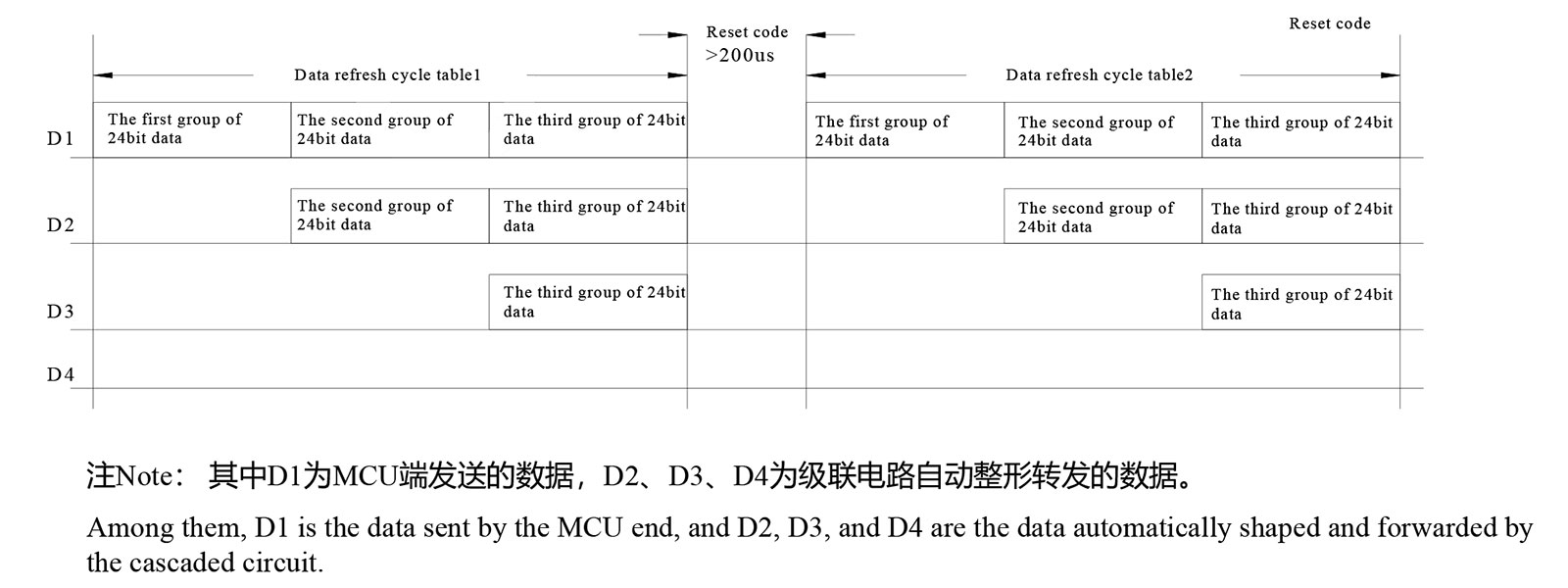
11. Data Transmission Method
12. Timing Waveforms
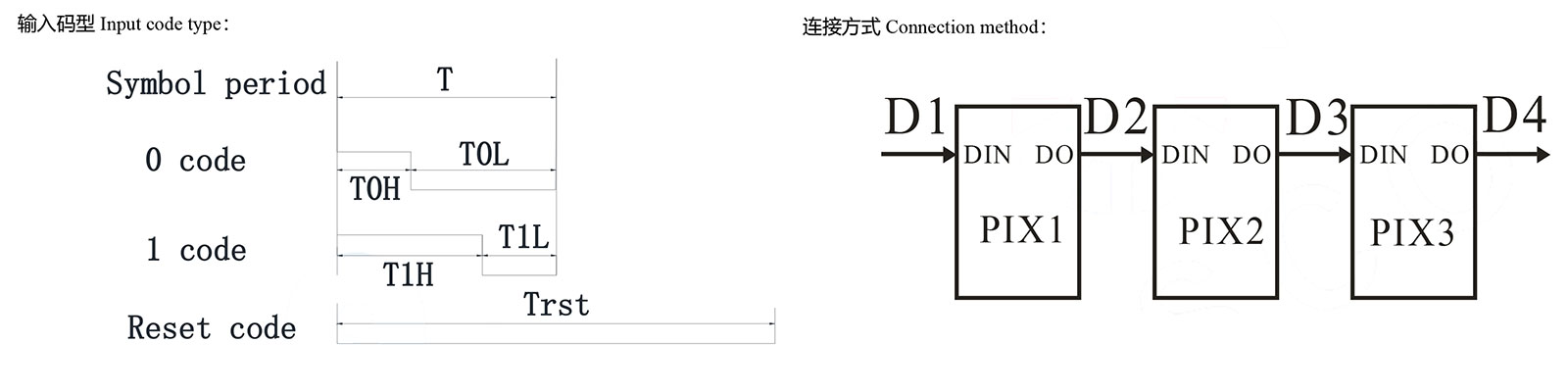
13. 24-bit Data Structure
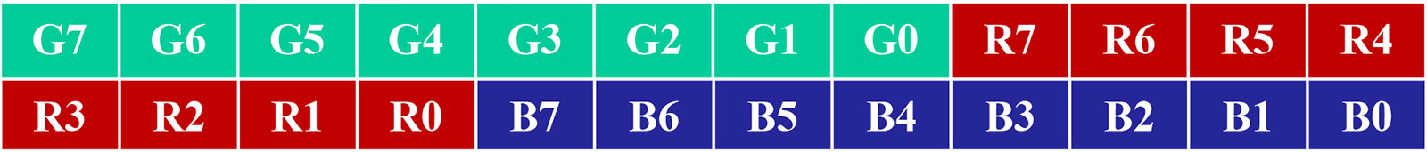
High bit is sent first. Data is transmitted in GRB order: G7 → … → G0, R7 → … → R0, B7 → … → B0.
14. Typical Application Circuit
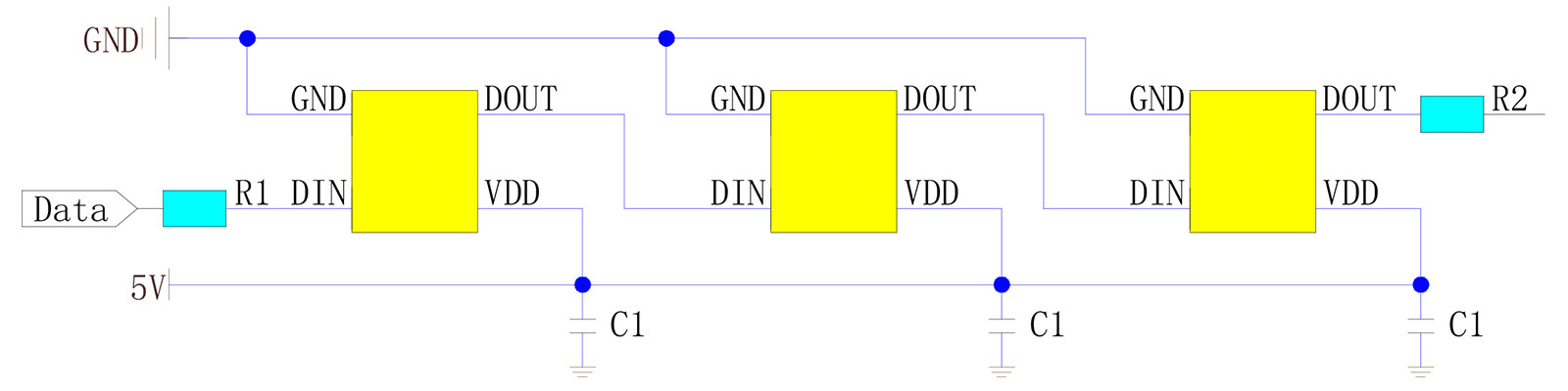
In practical circuits, to prevent instantaneous high voltage damage to the IC signal pins caused by hot-plugging during
testing, series protection resistors should be added at both the data input and output terminals.
Decoupling capacitors between each LED are essential for stable operation.
- Application 1: For soft or hard light strips with short distance between LEDs, use protection resistors
R1 and R2 of approximately 500 Ω at the signal input and output. The exact value should be determined by actual signal tests. - Application 2: For modules or general shaped products with longer transmission distance between LEDs,
the value of the series protection resistors depends on wire type and distance, and should be determined by actual usage.
15. Photoelectric Characteristics
The device exhibits typical relationships between pad temperature and relative luminous flux, wavelength characteristics,
and a typical radiation pattern of 120°. For detailed curves, refer to the original graphs:
- Relative luminous flux vs. pad temperature (RED / GREEN / BLUE)
- Relative spectral distribution vs. wavelength
- Typical radiation pattern (120°)
16. Packaging Standards
Surface-mount LEDs are supplied on reels, packed in anti-static bags, and then placed in cardboard boxes.
The cardboard box protects the LEDs from mechanical impact during transportation but is not waterproof.
Moisture-proof and waterproof measures should be taken during storage and handling.
- Reel size: 165/330 × 12 mm
- Each reel can hold up to 2000 / 8000 LEDs
- Anti-static polyethylene bag with desiccant and humidity indicator card
- Outer hard cardboard box, up to 20 bags per box
17. Reliability Testing
| No. | Test Item | Test Conditions | Reference Standard | Acceptance |
|---|---|---|---|---|
| 1 | Thermal shock | 100 ± 5°C ↔ -40 ± 5°C, 15 min / 15 min, 100 cycles | MIL-STD-202G | 0/22 |
| 2 | High temperature storage | Ta = +100°C, 1000 h | JEITA ED-4701 200 201 | 0/22 |
| 3 | Low temperature storage | Ta = -40°C, 1000 h | JEITA ED-4701 200 202 | 0/22 |
| 4 | High temperature and high humidity storage | Ta = 60°C, RH = 90%, 1000 h | JEITA ED-4701 100 103 | 0/22 |
| 5 | Temperature cycling | -40°C → 25°C → 100°C → 25°C, 30 min / 5 min / 30 min / 5 min, 100 cycles | JEITA ED-4701 100 105 | 0/22 |
| 6 | Resistance to soldering heat | Tsld = 260°C, 10 s, 2 times | JEITA ED-4701 300 301 | 0/22 |
| 7 | Normal temperature life test | 25°C, IF = typical current, 1000 h | JESD22-A108D | 0/22 |
Failure Criteria
| Item | Symbol | Test Conditions | Min. | Max. |
|---|---|---|---|---|
| Luminous intensity | IV | DC = 5 V, typical current | Initial value × 0.7 | — |
| Resistance to soldering heat | — | DC = 5 V, typical current | No dead LEDs or obvious damage | |